Technical

技術情報

Photolithography

Special technology to create ultra-fine and high-precision shapes
using "light" such as UV and X-rays

Photolithography is a technique for forming resin molds by irradiating (exposing) light on a photoresist (photosensitive resin) and developing it.
When a photomask is placed over the photoresist when irradiating with light, a photoresist with a shape that follows the pattern (two-dimensional figure) formed on the photomask is formed.
The important points in photolithography are " used light " and "irradiation technique".
By using our unique light irradiation technology such as X-ray irradiation, it can form resists of various shapes with unparalleled precision and sharpness.

Strengths of Optonics Precision's "Photolithography"

High dimensional accuracy

By using special light such as X-rays, it is possible to form a structure with excellent dimensional accuracy that cannot be achieved by conventional lithography.

Sharp shape

It is possible to obtain a shape with sharp edges and a smooth surface, which is difficult with other method of construction. Narrow pitch processing is also available.

Creation of 3D shape

With our unique irradiation technology, it is possible to create shapes that cannot be obtained by ordinary lithography, such as curved surfaces and multi-stage shapes.

Example of resist formation

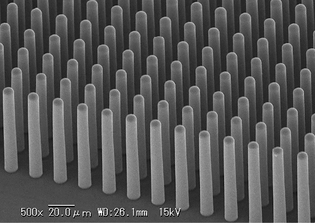
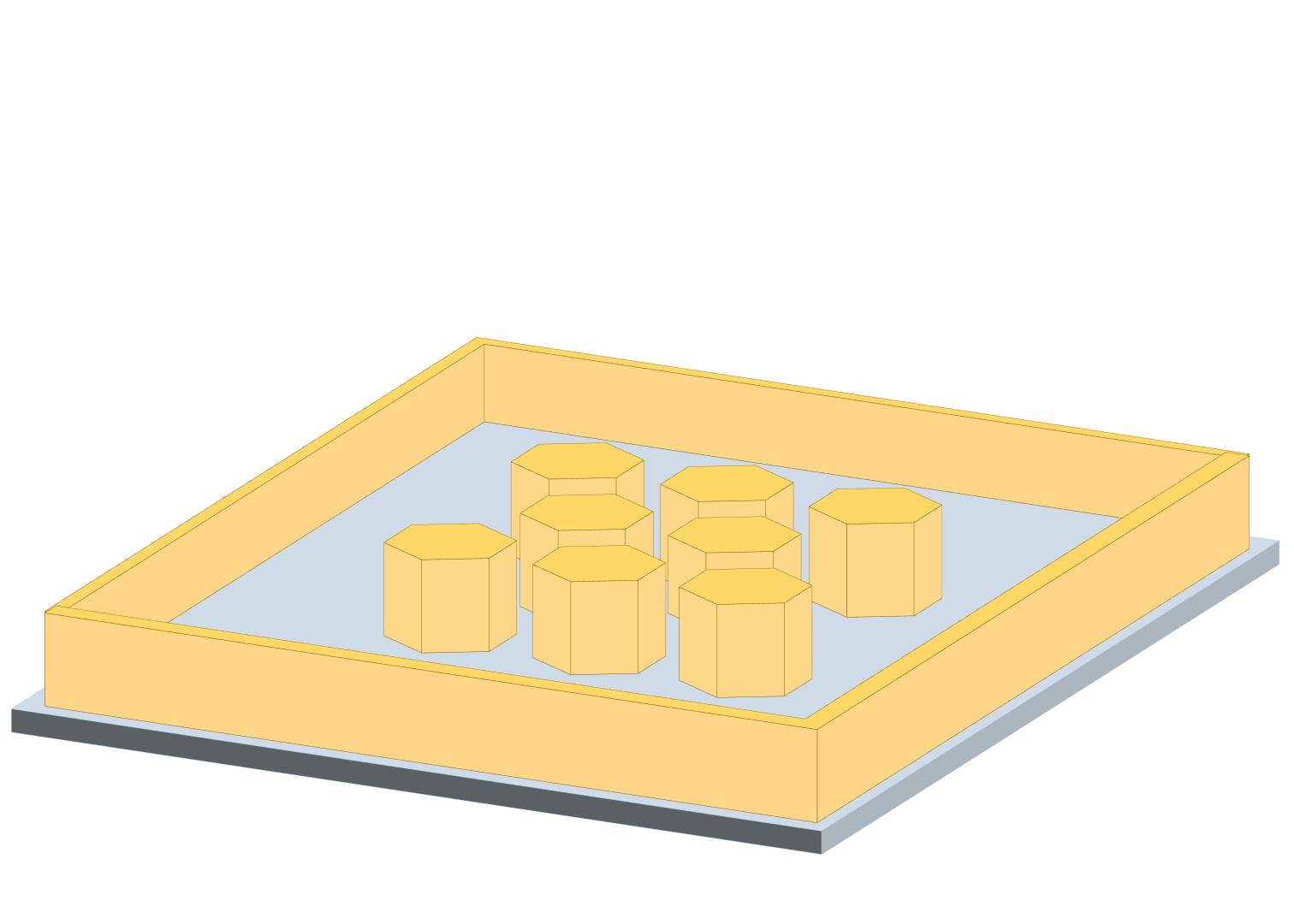
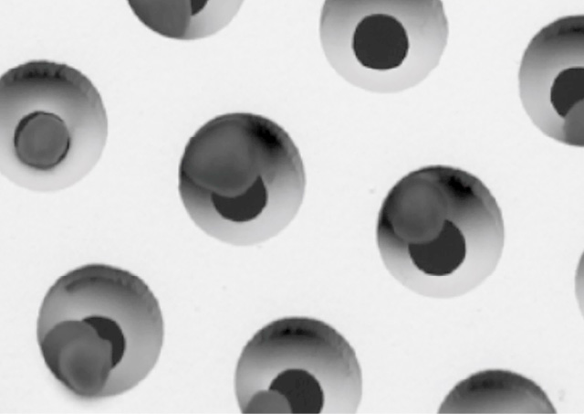
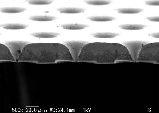
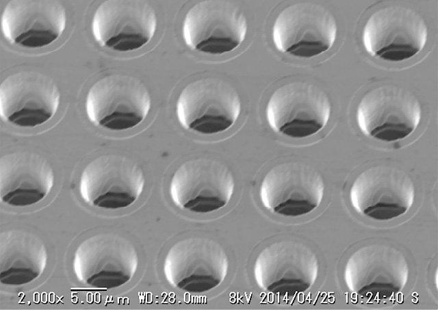
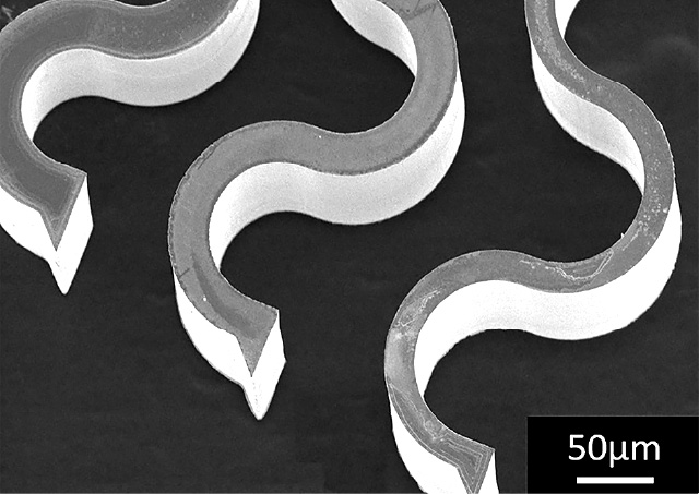
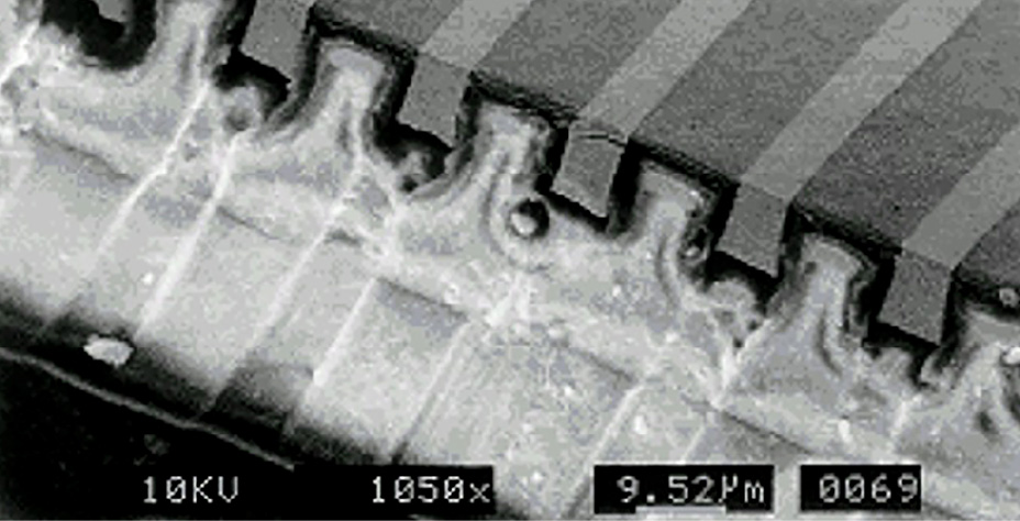
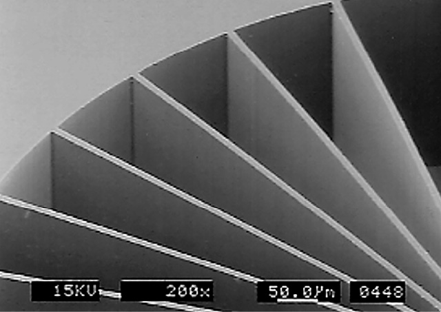
Pattern 1 thin wall structure

  • ■ Minimum wall width: 10 μm
  • ■ Wall height: 400 μm (aspect ratio = 400/10 = 40)

The wall structure with a high aspect ratio is formed without distortion.In addition, the edges are sharp and the side walls are smoothly formed.

Pattern 2 pillar array structure

  • ■ Pillar diameter: Φ10 μm
  • ■ Arrangement pitch: 20 μm
  • ■ Pillar height: 120μm (aspect ratio = 120/10 = 12)

Pillars with a high aspect ratio are formed with a narrow pitch.
The edges are sharp and the side walls are smoothly formed.
The pillars can be erected vertically or tapered.

Pattern 3 hemispherical array structure

  • ■ Sphere diameter: Φ20 μm
  • ■ Array pitch: 23 μm
  • ■ Sphere height: 10 μm

It is possible to form spherical shapes that are difficult to form with conventional photolithography, and the surface is finished smoothly.

Pattern 4 cone-shaped array structure

  • ■ Bottom side diameter: Φ500 μm
  • ■ Array pitch: 1500 μm
  • ■ Cone height: 700 μm

It is possible to form sharp-edged shapes that are difficult to form with conventional photolithography.

Pattern 5 multi-stage shape

  • ■ First step height: 200 μm
      〃Tip diameter: Φ100 μm
  • ■ Second stage height: 20 μm
      〃Tip diameter: Φ20 μm

It is also possible to provide a convex structure on the convex structure or a concave structure on the convex structure.

Electroforming

Metal precipitation technology using electrochemical reaction

Electroforming is a technique for depositing metal on a substrate while passing electricity through the conductive substrate in the electrolyte.
Electroform the substrate obtained by photolithography, then, the photoresist is removed and the precipitated metal layer is peeled off from the substrate to complete the product (metal thin film).
We synthesize the electrolytic solution by ourselves, and it is possible to create a metal with unique physical characteristics.

Electroformed product example

Electroformed product example 1: Corrosion resistant filter

  • ■ Material: Ni-based alloy ①
    Materials specializing in biocompatibility and cytotoxicity (chemical characteristics)

We have developed a Ni-based alloy that is biocompatible and has no cytotoxicity.
It is applied to cell filters. It can capture biological cells without killing them.

Electroformed product example 2: Nozzle for nebulizer device

  • ■ Material: Ni-based alloy ②
    Materials specializing in corrosion resistance and biocompatibility

e have developed a material that is corrosion resistant and biocompatible. It is applied to nozzles for nebulizer devices.
Nozzle constituent (metal ions) do not dissolve in the various sprayed liquids. It can be used safely

Electroformed product example 3: Printer-related parts

  • ■ Material: Ni-based alloy ③
    Material specialized for corrosion resistance

We have developed a material specializing for corrosion resistance that is applied to printer-related parts (nozzles, filters, etc.).

Electroformed product example 4: High elasticity probe

  • ■ Material: Ni-based alloy ④
    Material specialized for mechanical properties

We have developed a metal with high elasticity and excellent durability Applicable to inspection probe that expands and contracts repeatedly.

Electroformed product example 5: Various copper parts

  • ■ Material: Copper
    Material mainly intended to be non-magnetic

We provide various parts using copper for fields that require non-magnetism.

Electroformed product example 6: Various gold parts

  • ■ Material: Gold
    Material for X-ray blocking

We provide various parts using gold in the field of inspection and observation using X-rays.
Gold is also used for masks for X-ray lithography.

Other Technologies

Film-forming technology (dry, wet)

  • ・Dry: Vacuum deposition, sputtering
  • ・Wet: Electroplating, electroless plating

It is possible to add functionality by performing various film-forming on the product surface.

  • ・Water repellency
  • ・Corrosion resistance
  • ・Biocompatibility
  • ・Electrical insulation
  • ・Abrasion resistance
  • ・Reduction of contact (electrical) resistance, etc.

Frame processing technology

Our products are metal thin film parts. If it is difficult to use it as it is, it can be provided in the frame.
It is also possible to attach it to the frame or jig you provide, or we can propose a standard frame *.

* Example: Sieve (pasting a stainless-steel frame)
  Filter (attached to stainless steel frame)

Press microfabrication technology

This is a technique for drilling holes in metal thin films using a punch with a tip of 0.020 mm or less.
It can also be applied to materials such as stainless steel that cannot be processed by electroforming.
The hole diameter accuracy is equivalent to electroforming technology, and the shape is smooth.

Polishing technology

It is possible to suppress variations in product thickness and to remove protrusions on the product surface
Since scratches and burrs due to polishing are unlikely to occur, the quality of the product is not impaired.

Supports sizes up to 150x150 mm.

X-ray mask manufacturing technology

In X-ray lithography, we can manufacture masks (X-ray masks) to block X-rays.
By covering the resist with this mask, irradiating it with X-rays, and developing it, you can get sharp shapes that cannot be formed by conventional lithography.


  • ・X-ray absorber: Au (24K)
  • ・Membrane: Organic membrane (with visible light transmission)
  • ・Frame: Optional(We will design and manufacture according to the customer's request.)

Piezoelectric ceramic pasting technology

We will manufacture it as a spray element by laminating our electroformed mesh and piezoelectric ceramic.
We also support for mass production. It is also possible to attach it to the piezoelectric ceramic you supply, so please feel free to contact us.

Simple jig manufacturing technology by 3D printer

Using a 3D printer, it is possible to manufacture housings and frames for using electroformed products.
We can design it according to the customer's request, or we can only perform molding using the 3D data sent by the customer.
Please contact us for materials and available sizes.

Various evaluation techniques

The following evaluations can be performed in-company on the finished product.

  • ・ Mechanical property evaluation
  • ・Metal composition analysis (EDS)
  • ・Ion analysis in solution (ICP)
  • ・Reflectance evaluation
  • ・Surface roughness measurement
  • ・Contact angle measurement